Getting started with the Ebay's Kintex7 Accelerator

 YPCB-00388-1P1
To be honest, this week I had prepared another article about the carrier recovery algorithm. However, I received a board I bought some weeks ago on EBAY, and I was eager to try it out. The board is a PCIe FPGA accelerator based on the AMD Kintex7 XC7K480. It features almost half a million logic cells and over 1900 DSP slices. The cost of the board is less than 80 dollars. This is because it is not a new board, likely retired from some data center, but its status is practically new.

The board’s name is YPCB-00388-1P1, and the best part is that someone has documented the board quite good, creating a GitHub repository, and a webpage
To see what this board is capable of, we need to create a project. Since we have available the board files for this board, we just need to copy the files into our board repository. The board repository can be configured in the Vivado settings under “Tools > Settings > Project Settings > Board Repositories.” For more details, refer to this guide. Once configured, the board will be available in the Vivado project creation wizard.

Once the board is selected, we can continue creating the new project. The design we are going to create will be based on block design, so we need to create a new one. I always name the block design with the same name of the project, but adding the suffix _tb.
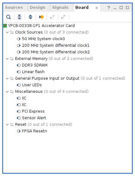
Once the block desing is created, we can find out that the board file also contain all the peripherals of the board, so we just need to add them in order to use them.
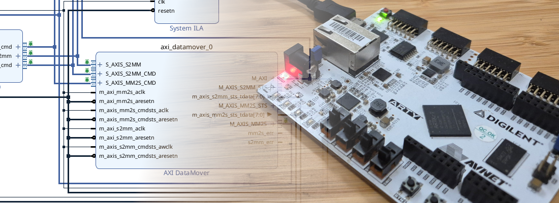
The board is designed to be used as a PCI accelerator, so it does not have any other external interface but PCI, so in the block design, the first IP we need to add is the PCIe interface. This part features GTX transceivers able to reach 12.5 Gbps. The board has 8 lanes connected to the PCIe gen2, and is this interface the one we are going to use to talk with the board. We have several options to include PCIe communication in our design. I am going to use the DMA/Bridge Subsystem for PCI Express IP, with is compatible with the XDMA drivers from AMD. If you don’t have them installed, in this article you can find a guide.
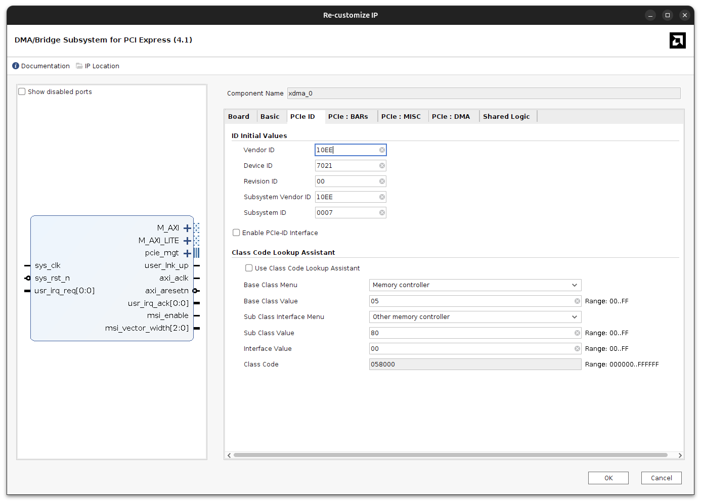
To make the host PC recognize the board as a XDMA driver compatible, we need to configure the IP following the next image.
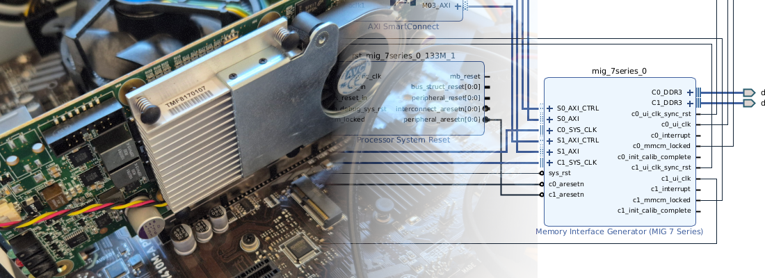
Once the PCIe IP is added, we can create a basic block design
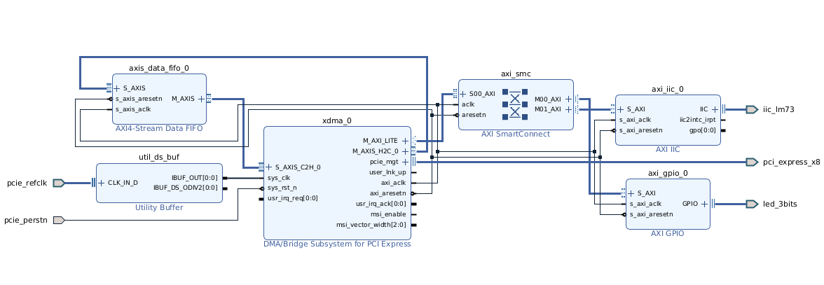
In the block design, the following components are configured:
- DMA/Bridge Subsystem for PCI Express: This is configured to implement an AXI4 Stream interface.
- AXI4 Stream Interface: Connected to a FIFO memory for efficient data transfer.
- AXI4 Lite Master: Connected to the AXI GPIO IP to manage the LEDs.
- AXI IIC IP: Connected to the LM73 sensor for temperature monitoring.
Board like this one democratize the use of big FPGA, and make them available for everybody, allowing small developers to have contact with parts that, in other context, would be inaccesible for them. The bad side is that, to create designs for this part, you need the Enterprise Edition of Vivado, which can be obtained as 1-month trial at no cost, but you will be limited to make all your work in one month. One of the reason I acquire this board, is because the project openXC7 support this FPGA, so it is a good idea to use it with this board.