Modeling a Boost converter in Speedgoat Performance.
It has been some since the last time we talked about Speedgoat, and during this summer I have been working with it deploying some models. In this blog we saw how to deploy a Buck converter electrical model using Speedgoat, this time we are going to deploy another converter model a Boost converter.
This converter is widely used for, for example, LED drivers, where we need to increase the voltage in order to connect different LEDs in series. Along this article, you will see how the steps to deploy different models are quite the same, and here is where is the power of Matlab and Speedgoat, if you know how to deploy one model, you know how to deploy any model.
The content of this article is the following:
- Simscape model
- FPGA Model
- Top model
- Simulink model simulation
- Generating the Space-State model
- HDL Workflow Advisor
- Real-time model deploy
- Conclusions
Simscape model
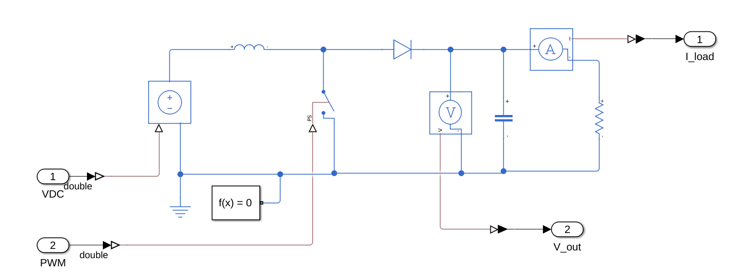
First of all, we are going to create the Simscape model of the boost converter. The system will be packaged in a hierarchical block, so we will need to add In and Out blocks to connect the hierarchical block. Notice that the PWM input, even being boolean, for Simscape is a floating point signal with double precision. The values of the currents and voltages will be also of type double.
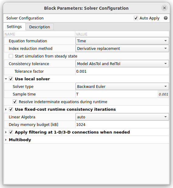
In the Simscape model, we need to add a Solver block. This block will be connected to the ground path. In the solver configuration, we need to configure to use a Local solver and set a timestep. I have used the variable T which will be defined later.
FPGA Model
Now, we need to create a hierarchical model with the Boost converter. The next is adding the gains for the IO334 board, and inserting a Signal Specification block on each port of the model. This will allow us later to change the data type from double to single, which is the format supported by the Speedboat target. This model will contain the design that, later, will be implemented in the IO334 board. At this level, the PWM input is a boolean signal, and the measure outputs will be 16-bit integers.

To connect the measures to the IO334 board, we need to apply a gain because the IO334 analog interfaces only allows to connect 16-bit signed signals. That gain depends on the maximum value the signal can take. For example, for the output voltage, since it is a Boost converter, it always will be greater than the input voltage, so we can mark a limit in 1000V. Since the output voltage of the IO334 is 10 volts for the maximum DAC value, the equation we must use is the next.
\[vout_{gain} = \frac{2^{15}}{vout_{MAX}}\]For the output current, since it is related to the output voltage by Ohm’s law, we know that the maximum output current is $Vout_{MAX}/R_{Load}$, so we can extract the gain as follows.
\[iout_{gain} = \frac{2^{15}}{vout_{MAX}/R_{Load}}\]We have to keep in mind that this model will be implemented in hardware, and the analog outputs will be connected to a Digital Analog Converter (DAC), so we will need to add a kind of Clock enable Signal for the DAC, the trigger. Since the Matlab version R2024a, we can keep this signal unconnected, and the DACs of the IO334 will be triggered synchronously with the model rate. On the other side, if we connect this signal to a constant ‘1’, the DAC will be configured to work in free run, this is, as fast as possible, event when the output of the model is not updated yet.
Top model
Finally, the top level will contain the FPGA model, and also the part of the model which will be executed in the processor of the Speedgoat target. Also, this model will be used to simulate the circuit since we can add the corresponding sources and scopes.

Before launching any simulation, we need to initialize all the variables of the model. For this model, the init.m script is the next.
close all
clear all
clc

% model parameters
L = 100e-6;
C = 330e-6;
Rload = 10;

T = 1e-6;

Fpwm = 20e3;
Tpwm = 1/Fpwm;

% gains for the IO334

dac_max_output = 10; % 10V
dac_bits = 16;

v_out_max = 1000;
v_out_gain = 2^(dac_bits-1)/v_out_max;

i_load_max = v_out_max / Rload;
i_load_gain = 2^(dac_bits-1)/i_load_max;
Notice that the top model, the one we will use for simulations, has two extra gains for the measures. Those gains are the inverse of the gains used to match the signals with the IO334 board. Those gains will convert the signal again into floating point values, so we will see looking into these signals the real values of the output voltage and the output current.
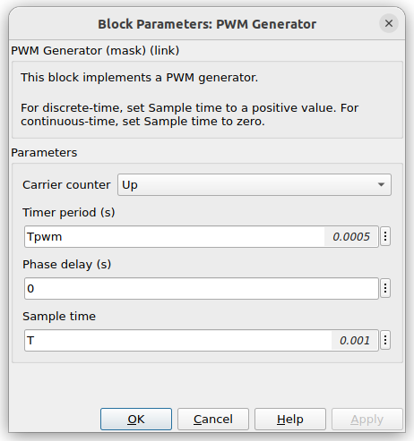
\[Kv = \frac{1}{vout_{gain}}\] \[Ki = \frac{1}{iload_{gain}}\]In the top model, we also can find a PWM signal generator. Although later the PWM input will be connected to an external input, it can be connected to a PWM generator for simulation purposes. Later this connection will be ignored. The configuration of the PWM signal generator is quite simple.
Simulink model simulation
In order to verify the correct behavior of the model, we are going to execute a simulation of the model in Simulink. The next figure shows the response of the system when the duty cycle of the PWM is 50%. The input voltage is set to 100 V so, ideally, the output voltage should be:
\[V_O = V_{IN} · \frac{1}{1-D}\]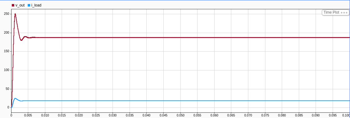
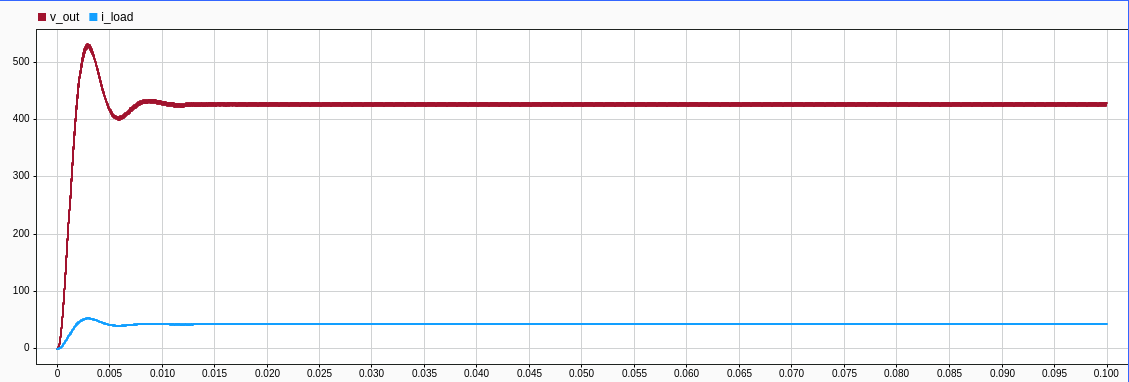
We can see that the output voltage does not reach the theoretical value. The reason is that the Boost model has some intrinsic resistances in the switches, besides the resistance of the inductor, so due to the current flow, some volts are lost. If we increase the duty cycle to 80%, although the output voltage is also increased, we can see that, due to the increment in the current, the losses are even larger.
Generating the Space-State model
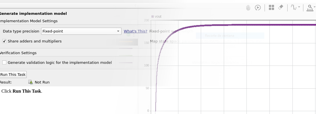
With these two points, we can see that the model works as expected, so we can now convert the Electrical model into a space-state model to be implemented in RTL. This can be done with the script model2ss.m, which sets some parameters of the HDL Coder, Set the number of the maximum iterations of the solver, and call the function sschdladvisor().
open_system('boost');

set_param(['boost/FPGA/boost/Solver Configuration'],'DoFixedCost','on')

set_param('boost', 'ProdHWDeviceType', 'ASIC/FPGA->ASIC/FPGA')

% Set number of solver iterations
set_param('boost/FPGA/boost/Solver Configuration','MaxNonlinIter','2')

hdlsetup("boost")

% Launch SS HDL advisor
sschdladvisor('boost')
Once the Simscape HDL Advisor is open, we can execute all the steps.
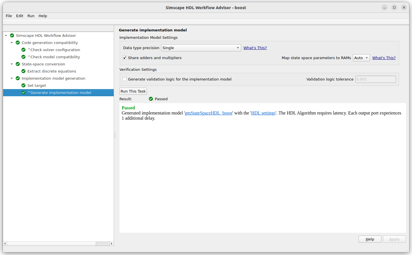
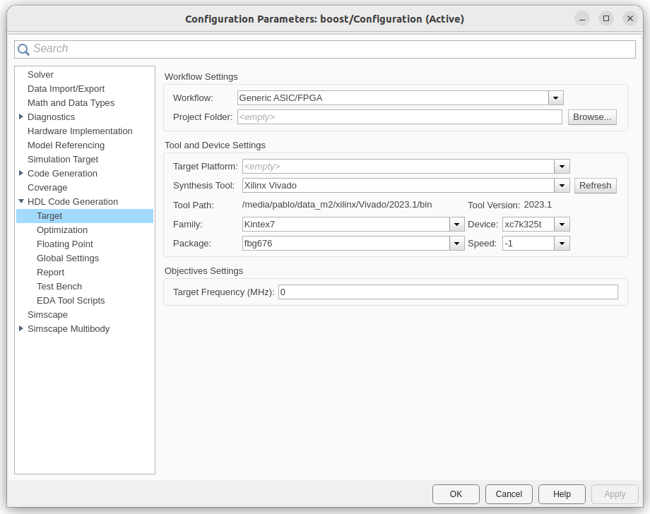
Some versions ago, the Simscape HDL Advisor returned an error if the target device was not configured. In this case, you can navigate to the HDL Coder option, and set the Device Settings.
This new model can also be simulated to ensure that the conversion has not broken the model. In addition to the Simulink model, a .mat file is also generated. IN this .mat file you will find all the space state parameters. Once we make sure that the models work correctly, we can launch the HDL Workflow Advisor to generate the FPGA design of the converter.
HDL Workflow Advisor
The following script adds to the path the VIvado installation used for this model. Also, changes the signal data type of all the Signal Specification blocks from double, used for the simulation, to single, which is the type that the FPGA model can manage. Finally, calls the function hdlsetup, which configures the HDL Coder, and launches the HDL Workflow Advisor with the command hdladvisor.
hdlsetuptoolpath('ToolName','Xilinx Vivado','ToolPath','/media/pablo/data_m2/xilinx/Vivado/2023.1/bin/vivado');

open('./sschdl/boost/gmStateSpaceHDL_boost.slx')

set_param('gmStateSpaceHDL_boost', 'SimulationCommand', 'Update')

set_param('gmStateSpaceHDL_boost/FPGA/Signal Specification','OutDataTypeStr','single');
set_param('gmStateSpaceHDL_boost/FPGA/Signal Specification1','OutDataTypeStr','single');
set_param('gmStateSpaceHDL_boost/FPGA/Signal Specification2','OutDataTypeStr','single');
set_param('gmStateSpaceHDL_boost/FPGA/Signal Specification3','OutDataTypeStr','single');

hdlsetup('gmStateSpaceHDL_boost')

hdladvisor('gmStateSpaceHDL_boost/FPGA')
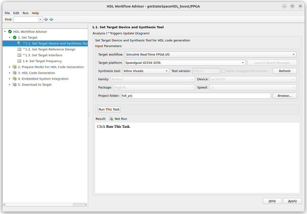
When the HDL Workflow Advisor is open, we need to configure as Target workflow the option Simulink Real-Time FPGA I/O, then, in the Target platform, we will select the Speedgoat IO334-325k. The other options will be filled automatically.
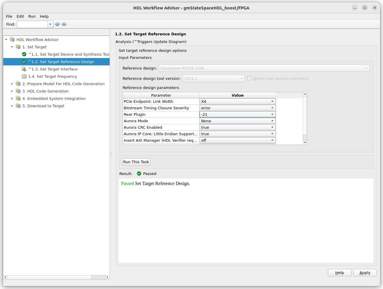
In step 1.2 Set Target Reference Design, we need to configure the IO334. In my case, I have connected the Rear Plug-in -21. The other options can be left as default.
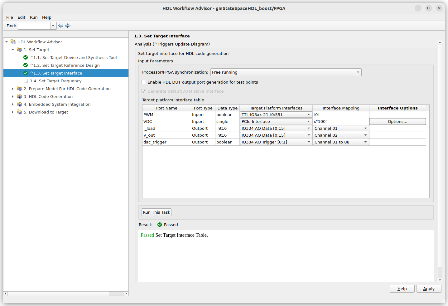
Now we need to connect the ports of the mode to the ports of the Speedgoat Target. For the inputs, the PWM signal will be connected to a digital input, and the VDC value will be configured through the PCIe interface, in other words, the microprocessor will configure the VDC voltage according to the value configured in Simulink. Regarding the outputs of the models, both measures will be connected to AO Data channels, and the trigger output will be connected to the AO Trigger output.
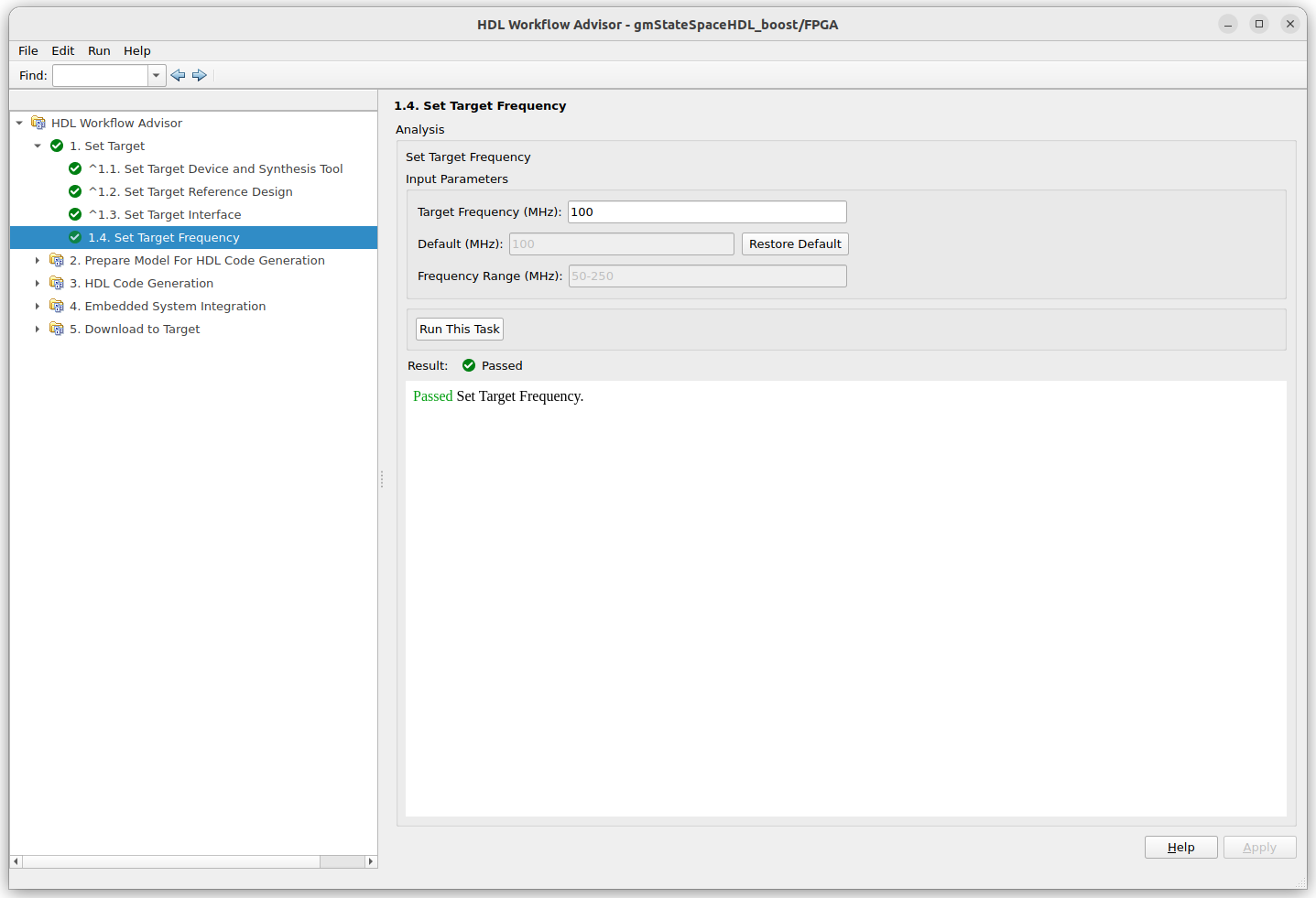
In the next step, we need to set the frequency of the main clock of the FPGA. This configuration will determine the final time step of the model. This time step can be calculated as:
\[Ts = \frac{SYSCLK}{OversamplingFactor \cdot SolverIterations}\]Since a smaller time step will result in a better simulation, we can be tempted to increase the target frequency but in many cases, frequencies above 150 or 200 MHz will result in timing issues in the final implementation of the FPGA. If we need to decrease the time step of the model, the oversampling factor can be reduced in the HDL Coder options.
After the target frequency configuration, we can go to step 3.2, and run all the steps until this one. In step 3.2, the HDL code will be generated, and a report with all the configurations taken for the generation.
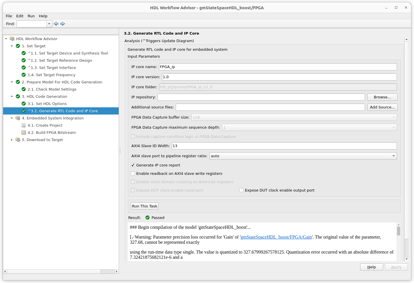
Finally, we can generate the Vivado project, and generate the bitstream. During the bitstream generation, unlike the IP Core Generation workflow, we won’t see any output, so we will wait until this step is finished.
The last step of the workflow is the generation of the integration model. This model will connect the Speedgoat target, and it will be the code that will run in the microprocessor of the Speedgoat target.
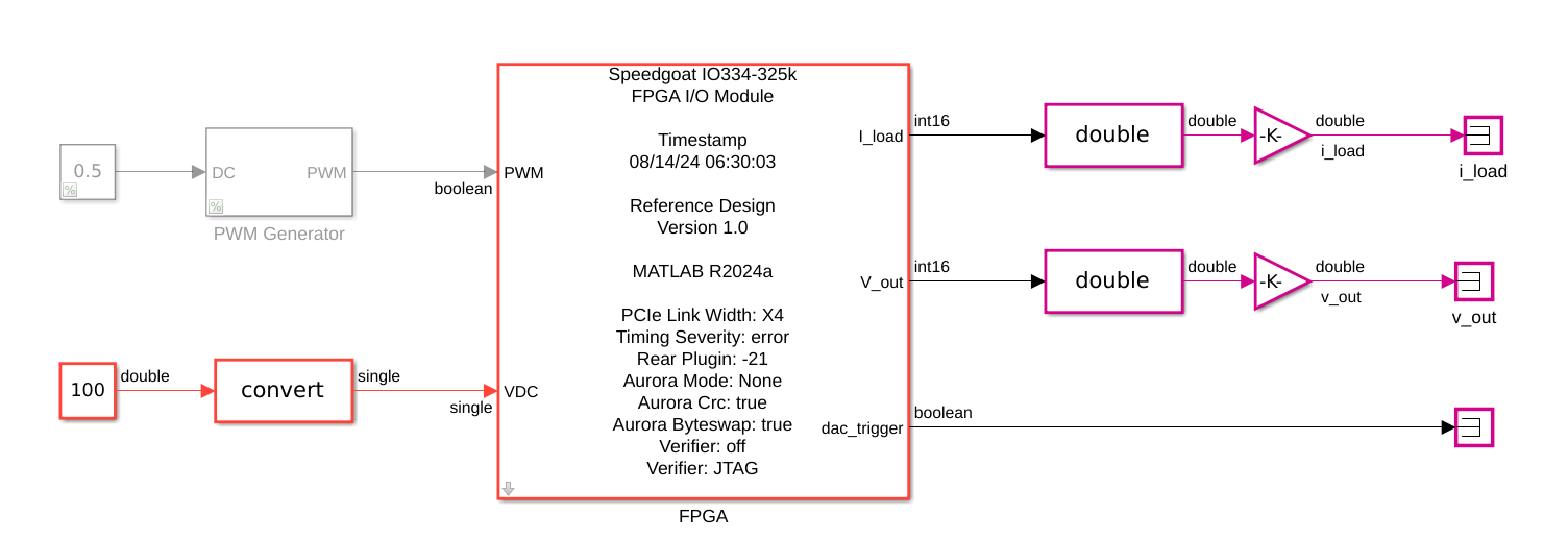
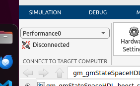
Within this model, we can connect with the Speedgoat target.
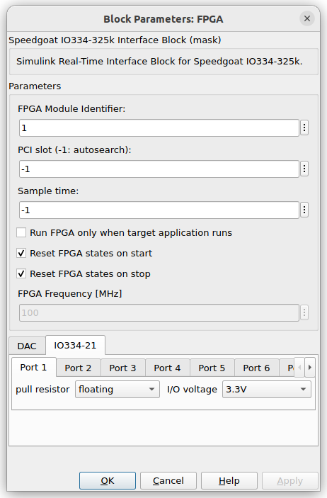
In the integration model, we can also configure some aspects of the IO334 board such as the digital IO voltage and the analog output range.
Real-time model deploy
At this point, we are ready to send and deploy the model in the Speedgoat target, just one step left. The timestep of the simulation is set to 1us. This configuration was been configured for the Simulink simulation. If we keep this value, the Speedgoat microprocessor will try to keep that time step in the real-time simulation, which is almost impossible for a microprocessor that is running an OS, so we will need to change the timestep to 50us. This time step won’t change the time step of the model running in the FPGA, since it is already set according to the target frequency, the oversampling, and the solver iterations, it just will modify the timestep of the part of the model running in the microprocessor which, in our case, it is just the VDC value sending over PCIe.
Once the time step has been changed, we can run the model. I have run two different tests on this model. The first one, I have connected an FPGA to the digital input board generating a PWM signal of 80% at 2 kHz.
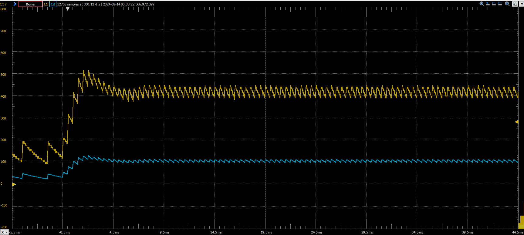
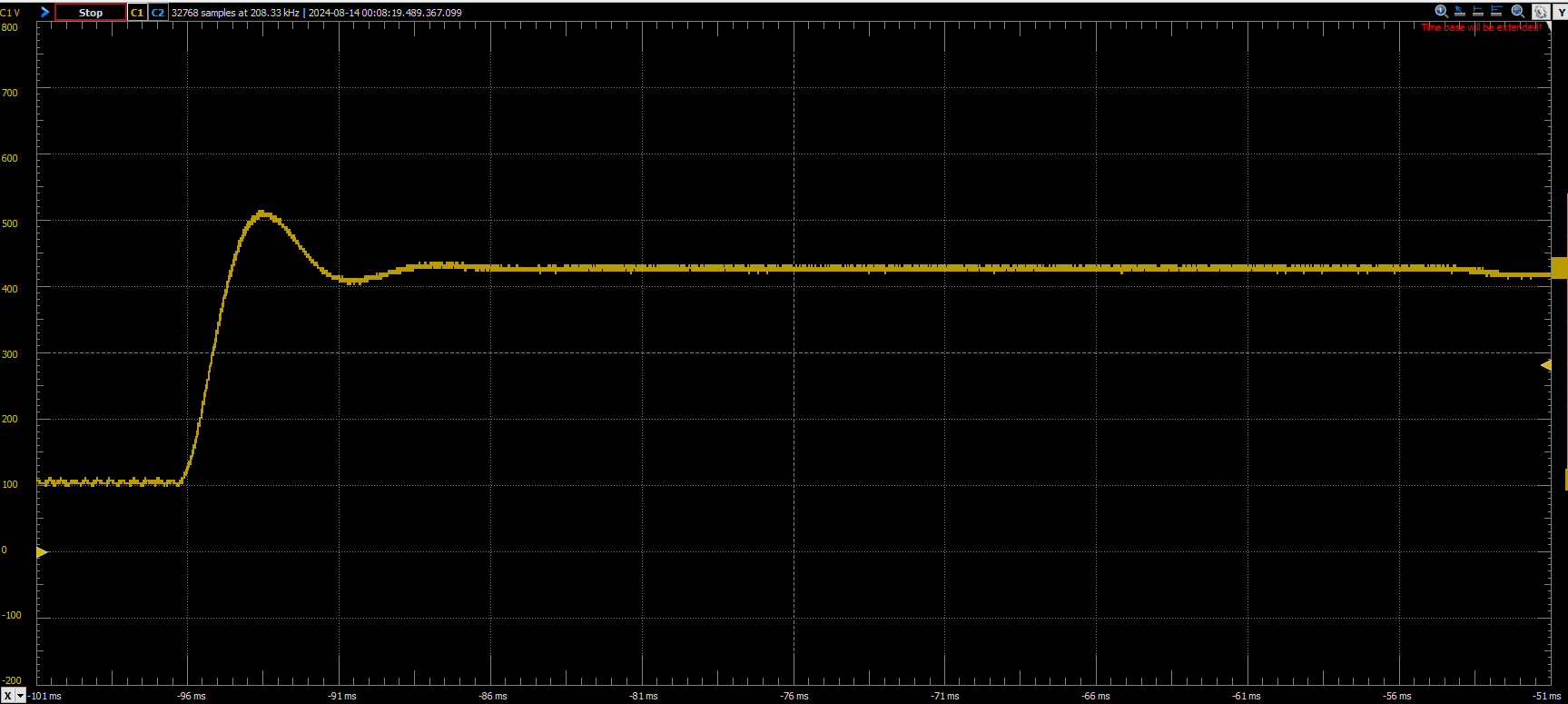
We can see the ripple of the output voltage with a frequency of 2 kHz. If I increase the PWM frequency to 20 kHz, the ripple is reduced, which is the expected behavior.
Conclusions
Although with some differences, you will notice that the deployment of any model follows the same steps as the Buck model, with the difference that, for the Buck deployment I had a Speedgoat Baseline, and now I have a powerful device, the Speedgoat Performance Device, which also demonstrates that, for different models, and even different targets, the deployment of electrical models are pretty similar.


