Adding custom RTL modules to an electrical model
Tools like Matlab and Simulink offer engineers a bunch of packages to do their jobs. As FPGA developers, the packages that, in some cases, could make our designs faster to develop are HDL Coder and HDL Verifier. In addition, if we mix those packages with compatible hardware like the Speedgoat Performance, we can develop projects in weeks instead of months. As an FPGA developer, developing HDL code using HDL coder could help in some cases, but there are applications where is easier and faster to write a Verilog code instead of describing the module in a Simulink model. In this case, we can multiply the power of those tools by integrating both, code generated by HDL coder, and also code generated by us in the same model. In this article, That is just what we are going to do.
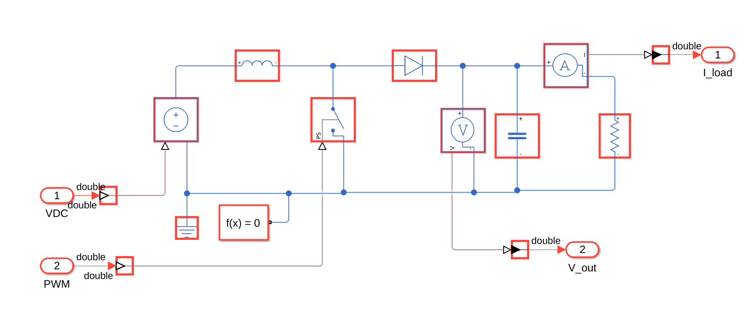
As a base model I am going to use the Boost converter model deployed in the Speedgoat device in this article, and then we will replace the PWM input with a PWM signal generator module written in Verilog, so the HDL Coder will integrate our HDL module into the Simulink model.
This article has the next points:
- Simscape model
- FPGA Model
- Generating the Space-State model
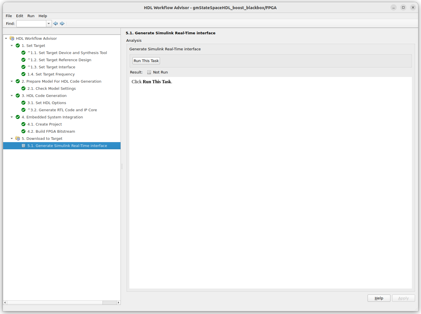
- HDL Workflow Advisor
- Real-time model deploy
- Conclusions
Simscape model
The Simscape model I am going to use, as I said before, is the Boost model.
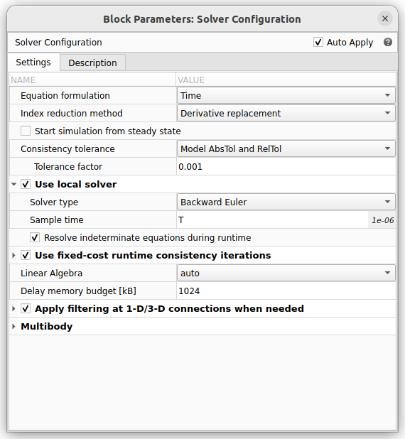
We will need to change the solver configuration setting the option Use local solver, and configuring the Sample Time as T, which will be defined later.
Now we will create the FPGA model which contains the Boost model, and all the blocks needed to communicate with the IO334 board.
FPGA model
At this point, we have a model similar to the one deployed in the original article. Now, we need to replace the PWM input with this PWM generator designed in Verilog.
`define S_AXI_DATA_WIDTH 32

module pwm (
	input wire aclk,
	input wire reset,
	input wire clk_enable,

	/* Configuration */
	input wire [`S_AXI_DATA_WIDTH-1:0] pwm_period,
	input wire [`S_AXI_DATA_WIDTH-1:0] pwm_comparator,
	output reg [`S_AXI_DATA_WIDTH-1:0] pwm_counter,

	/* PWM output*/
	output reg pwm
);

	/**********************************************************************************
	*
	* PWM Sawtooth generator
	*
	**********************************************************************************/
	always @(posedge aclk)
		if (reset)
			pwm_counter <= 0;
		else
			if ((pwm_counter >= pwm_period))
				pwm_counter <= {`S_AXI_DATA_WIDTH{1'b0}};
			else
				pwm_counter <= pwm_counter + 1;

	/**********************************************************************************
	*
	* Output signal comparator
	*
	**********************************************************************************/
	always @(posedge aclk)
		if (reset)
			pwm <= 1'b0;
		else
			if (clk_enable)
				pwm <= (pwm_counter < pwm_comparator)? 1'b1: 1'b0;
endmodule
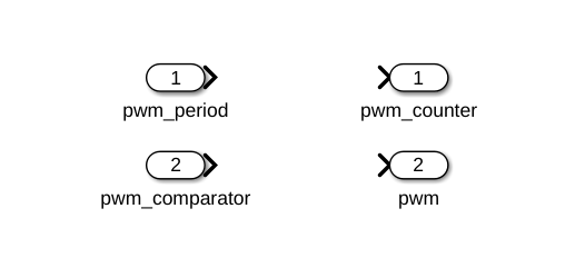
To do this, we need to use a blackbox that will implement the HDL design. To create a blackbox, we are going to add the same In and Out blocks that our HDL design has, except clock, reset and clock enable.
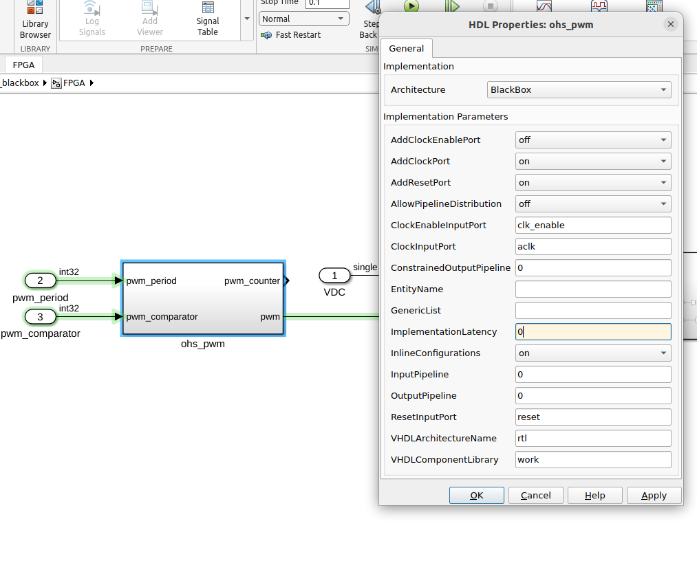
Now, we will group all the IN and OUT blocks within a hierarchy block and then we can configure that block as a Blackbox. We can open the configuration menu by doing right click on the HDL block, and clicking on HDL Coder > HDL properties. In the window that will be opened, in the Architecture configuration we must select Blackbox, and configure the name of the clock, reset and clock enable ports. Notice that the module I have designed uses a non-negate reset, which is the reset type used later in the Vivado project.
The hierarchy block created must be named as the name of the Verilog module, to allow the HDL coder to make the connection between the HDL module and the block.
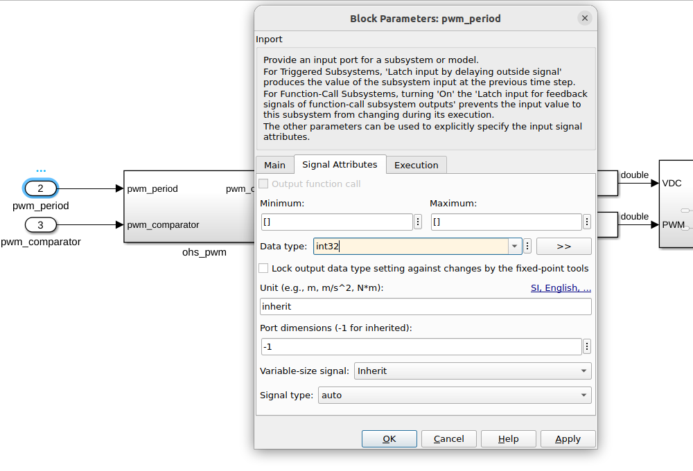
The next step is to change the data type of the ports of the blackbox. We need to match the type of the port and the type declared in the HDL code. In this case, pwm_period and pwm_comparator will be configured through the PCIe interface of the Speedgoat target, so they need to be declared as 32-bit integers. The module has two different outputs, the PWM itself, which is a 1-bit signal or boolean, and the second output is the value of the counter, which will be connected to the PCIe interface, so it needs to be declared as 32-bit integer.
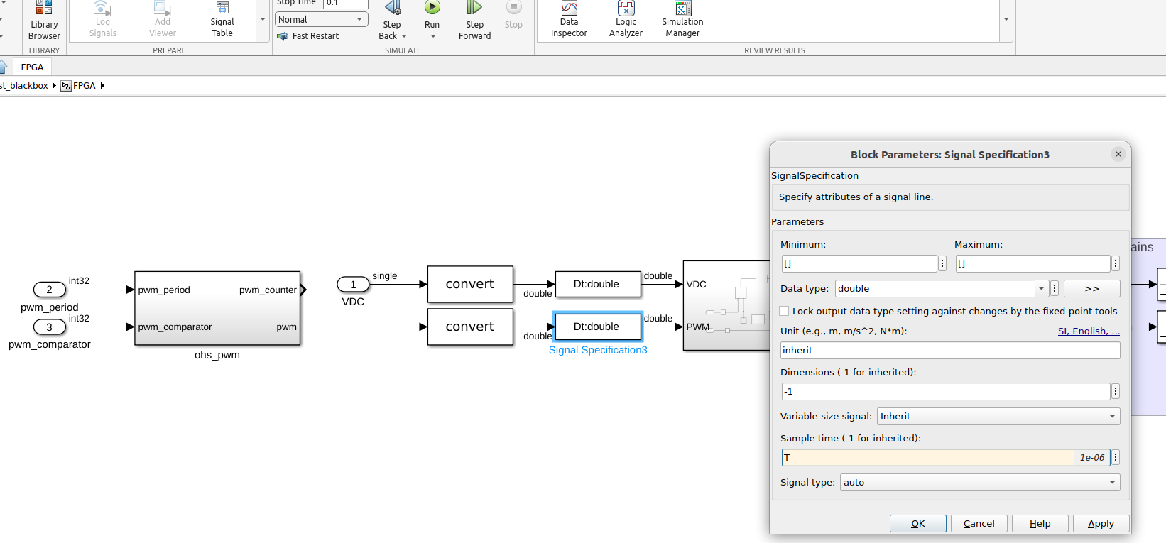
Finally, since all the source blocks must have a timestep defined, and we can not define the time step of the blackbox, we can define the time step in the Signal Specification block. This will ensure that all the model runs at the same time step, and avoid future errors in the HDL Workflow Advisor.
Done this, we can complete the top model. To simulate this model, since we can’t integrate the RTL code in the Simulink simulation, we can add a model within the blackbox that replaces the RTL code. This way we will be able of simulating the entire model to verify the behavior of the generated model.
Generating the Space-State model
To generate the RTL model of the Boost, we can use the script model2ss.m, which sets some parameters of the HDL Coder, Set the number of the maximum iterations of the solver, and call the function sschdladvisor().
open_system('boost');

set_param(['boost/FPGA/boost/Solver Configuration'],'DoFixedCost','on')

set_param('boost', 'ProdHWDeviceType', 'ASIC/FPGA->ASIC/FPGA')

% Set number of solver iterations
set_param('boost/FPGA/boost/Solver Configuration','MaxNonlinIter','2')

hdlsetup("boost")

% Launch SS HDL advisor
sschdladvisor('boost')
Once the Simscape HDL Advisor is opened, we can execute all the steps.
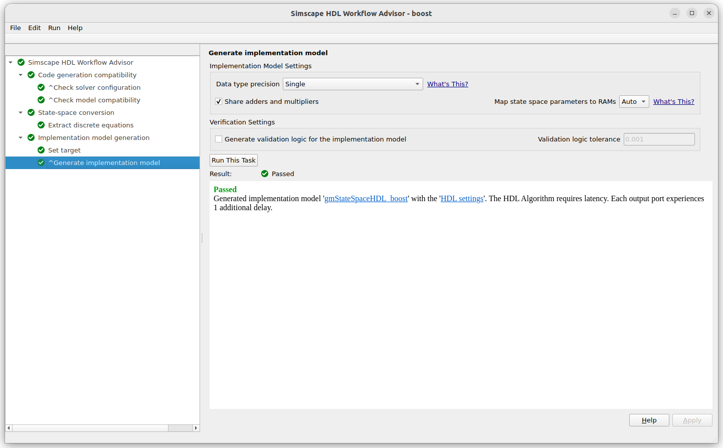
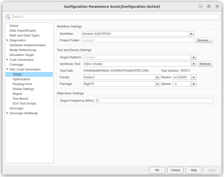
Since some versions ago, the Simscape HDL Advisor returns an error if the target device is not configured. In this case, you can navigate to the HDL Coder option, and set the Device Settings.
HDL Workflow Advisor
The following script adds to the path the Vivado installation used for this model. Also, changes the signal data type of all the Signal Specification blocks from double, used for the simulation, to single, which is the type that the FPGA model can manage. Finally, calls the function hdlsetup, which configures the HDL Coder, and launches the HDL Workflow Advisor with the command hdladvisor.
hdlsetuptoolpath('ToolName','Xilinx Vivado','ToolPath','/media/pablo/data_m2/xilinx/Vivado/2023.1/bin/vivado');

open('./sschdl/boost/gmStateSpaceHDL_boost.slx')

set_param('gmStateSpaceHDL_boost', 'SimulationCommand', 'Update')

set_param('gmStateSpaceHDL_boost/FPGA/Signal Specification','OutDataTypeStr','single');
set_param('gmStateSpaceHDL_boost/FPGA/Signal Specification1','OutDataTypeStr','single');
set_param('gmStateSpaceHDL_boost/FPGA/Signal Specification2','OutDataTypeStr','single');
set_param('gmStateSpaceHDL_boost/FPGA/Signal Specification3','OutDataTypeStr','single');

hdlsetup('gmStateSpaceHDL_boost')

hdladvisor('gmStateSpaceHDL_boost/FPGA')
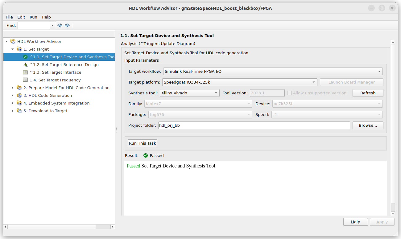
When the HDL Workflow Advisor is open, we need to configure as Target workflow the option Simulink Real-Time FPGA I/O, then, in the Target platform, we will select the Speedgoat IO334-325k. The other options will be filled automatically.
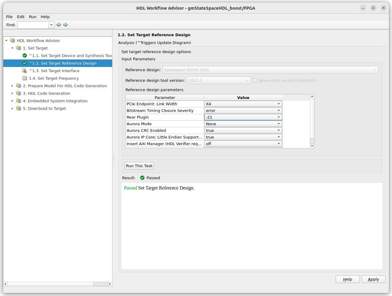
In step 1.2 Set Target Reference Design, we need to configure the IO334. In my case, I have connected the Rear Plug-in -21. The other options can be left as default.
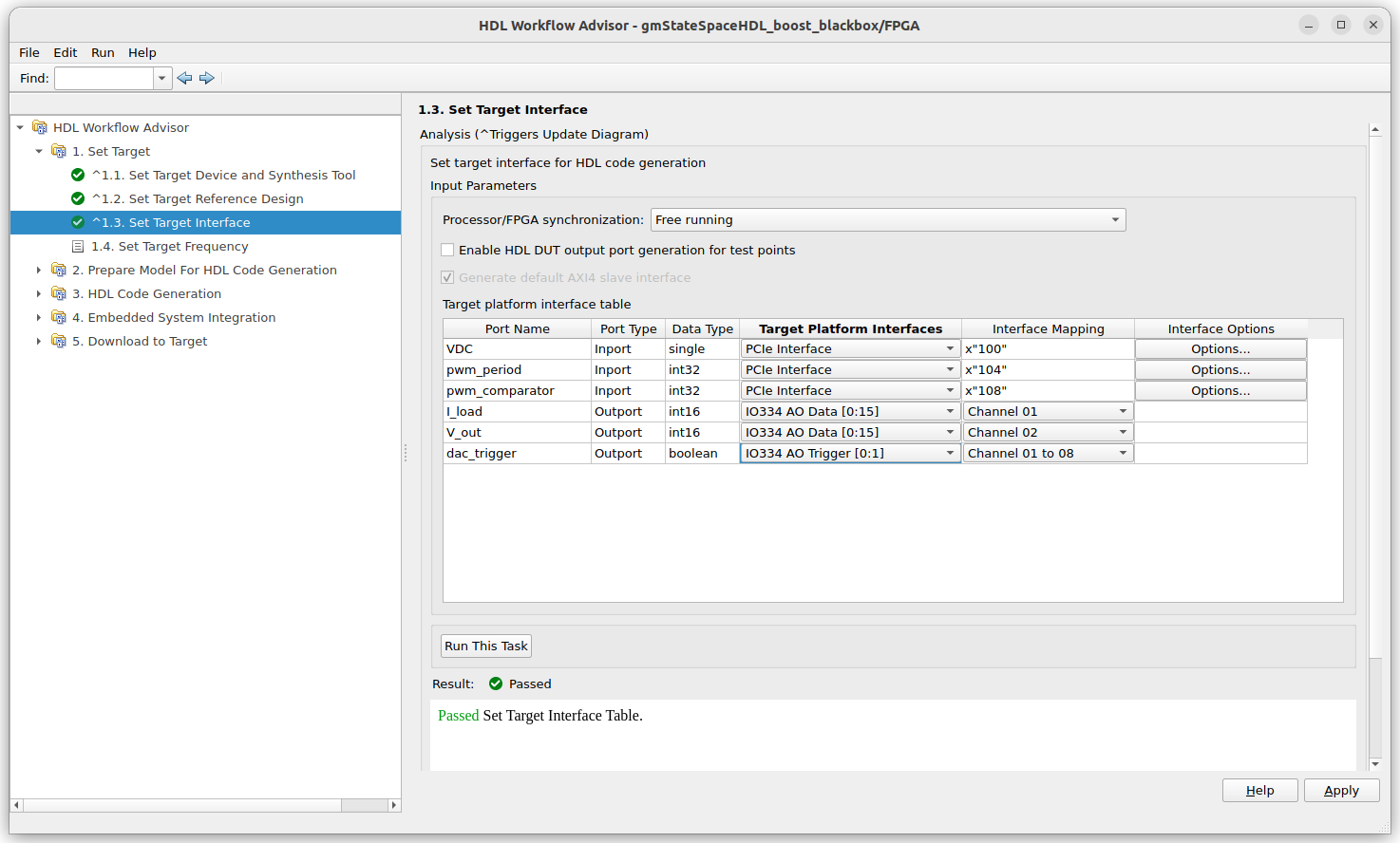
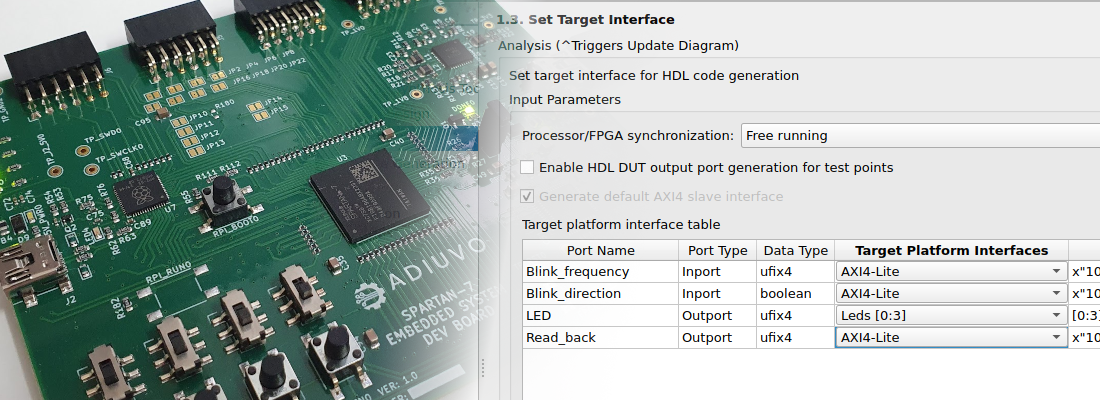
Now, this step differs from other articles. In the configuration of the interface, we do have not a PWM input, we will have the inputs of the HDL module added as a blackbox instead. These inputs will be connected to the PCIe Interface since we will configure them through the Simulink integration model. The analog output signals will be connected to the interface AO Data, the DAC trigger to the AO Trigger, and the VCD to the PCIe Interface.
Now you can jump tot he step 3.2. In this step, you have to add the HDL files needed to create the project. In this case, we have to add the file that contains the module pwm. Then, we can run all the steps until this one.
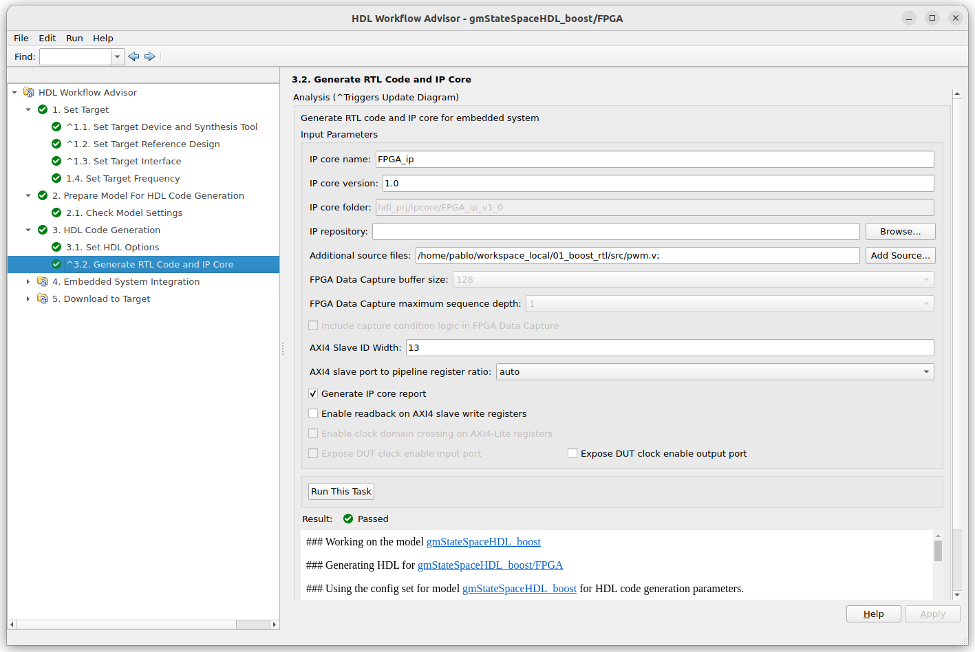
In the report generated in this step, you can see that the module has been added as a blackbox, as well as all the configuration parameters of the model like VDC or the HDL module inputs.
The next is to generate the Vivado project. In this project will be added all the Speedgoat target modules in addition to the module we have created.
When the project is generated, is interesting to open the project and verify how HDL Coder has connected the module with all the rest of the modules. The Vivado project is located at hdl_prj_bb/vivado_ip_prj/.
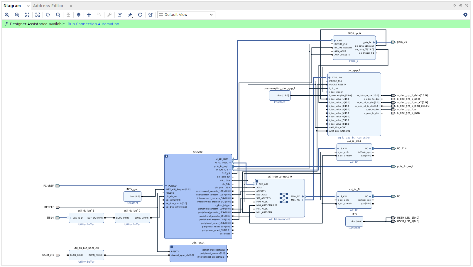
In the block design of the project, we can see some modules needed for the IO334 management like the PCIe interface.
Throughout these blocks, we are going to open the code of the FPGA_ip block. This block implements the FPGA hierarchy block of the Simulink. Within this block, we can find the power converter, the gains for the IO334 analog outputs, and the instantiation of the PWM module.
pwm u_pwm (.aclk(clk),
	.reset(reset),
	.clk_enable(clk_enable),
	.pwm_period(period),  // uint32
	.pwm_comparator(comparator),  // uint32
	.pwm_counter(pwm_out1),  // uint32
	.pwm(pwm_out2)  // uint32
	);

...

FPGA_ip_src_boost u_boost (.clk(clk),
		.reset(reset),
		.enb(enb),
		.enb_1_2500_0(enb_1_2500_0),
		.enb_1_2500_1(enb_1_2500_1),
		.VDC(VDC),  // single
		.PWM(Data_Type_Conversion2_out1_2),  // single
		.sch_ctr_4999(s),  // ufix13
		.I_load(boost_out1),  // single
		.V_out(boost_out2)  // single
		);
We can also verify how the HDL Coder has connected the PWM output of the HDL module with the PWM input of the converter. The wire that connects both ports is Data_Type_Conversion2_out1_2. Simscape works just with floating point signals, so the PWM input of the converter will be a signal of type Single. Since the PWM output of the pwm HDL module is boolean, the HDL Coder transforms this boolean signal into a floating point signal.
assign Data_Type_Conversion2_out1 = 32'h00000000;

assign Data_Type_Conversion2_out1_1 = 32'h3f800000;

assign Data_Type_Conversion2_out1_2 = (pwm_out2 == 1'b0 ? Data_Type_Conversion2_out1 :
						Data_Type_Conversion2_out1_1);
Notice that the value of Data_Type_Conversion2_out1_1 is corresponding with ‘1’ in the floating point. Now, coming back to HDL Coder WFA, we can build the bitstream.
To be able to debug the RTL module, I have changed the Simulink model to connect the PWM signal to a digital output and a PWM counter to an analog output.
Finally, we can generate the interface model, which will be used to manage the inputs of the Verilog module.
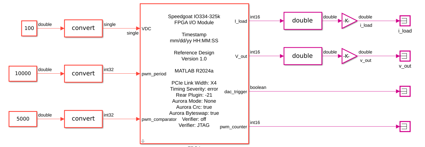
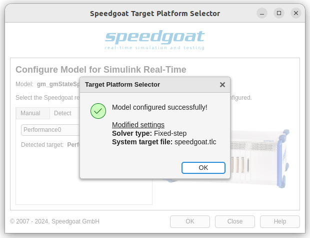
Once all the steps are finished, we can connect the Speedgoat Performance Target. To do this, we have to open the Speedgoat Target Platform Selector and detect the device that is connected to the host computer.
When the device is selected, we need to click on OK to apply the correct configuration to the model.
Real-time model deploy
Before deploying the model in the Speedgoat target, we need to change the Timestep for the simulation from 1us, used for the model generation, to 50us, a time step that the target microprocessor can handle. With this change applied, we can deploy and run the model.
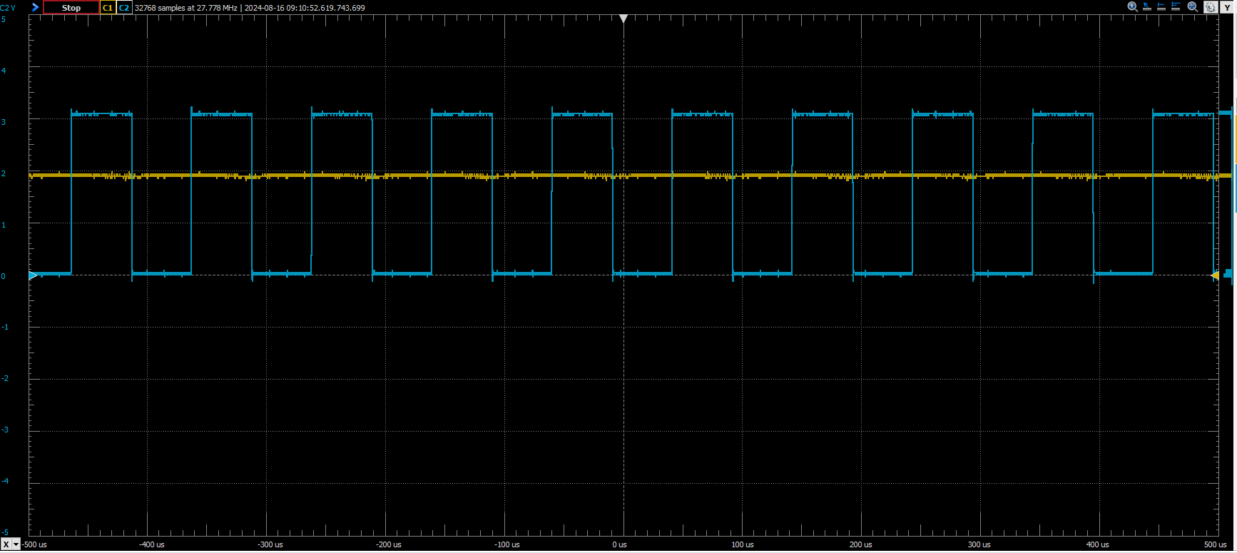
The response of the model is the next. We can see the PWM output and the output voltage. The Boost converter is connected to a 100V source, that corresponds with a 1-volt output. Since the PWM duty cycle is 50%, the input voltage is doubled at the output, obtaining 200V, which corresponds with 2 volts at the output.
Conclusions
The Speedgoat Performance device is a complex device with different architectures inside. In my job, we have several hardware-in-the-loop targets used by the embedded SW developers team who view the device as a Simulator, which is exactly what it is, but from the point of view of an FPGA developer, the Speedgoat Performance Device is a host computer with an FPGA acceleration board connected over PCIe. This acceleration card features several digital-to-analog converters (DAC), Digital IN/OUT, and high-speed interfaces… all of this makes this device very interesting for us. In this article, you have seen how, in the final step of the HDL Coder Workflow Advisor we have a regular Vivado project, and is here where we, FPGA developers are very comfortable.


