Deploying a Buck-Boost model on a custom HIL platform.
A few years ago, I found the hardware-in-the-loop (HIL) platform to be very interesting. I am sure that you have noticed this because of all the articles I write about these platforms and modeling. What makes interesting for me these platforms is that they mix all the electronic fields I like, power electronics, digital signal processing, and FPGA. If you follow my social networks you will know that I am working on a project to create an open HIL platform. The first step was to create some models, and now you can find in this blog models for Buck and Boost converters. So, the next is to create the hardware platform, and it is almost done with the Platform Board. This board is intended to be the base for the first steps of the project. In this article, we are going to test this board with a new model.
The model we will use is the Buck-Boost converter. This converter is able to both step-up and step-down the input voltage in its output. Another particularity of this converter is that the output is inverted, so it is widely used to generate negative voltage rails. The transfer function of the ideal Buck-Boost converter is the next:
\[V_O=V_{IN} \cdot \frac{-D}{1-D}\]where D is the duty cycle.
The diagram of the convertes is shown in the next figure.
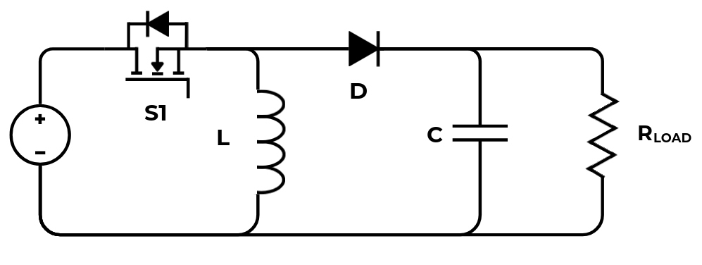
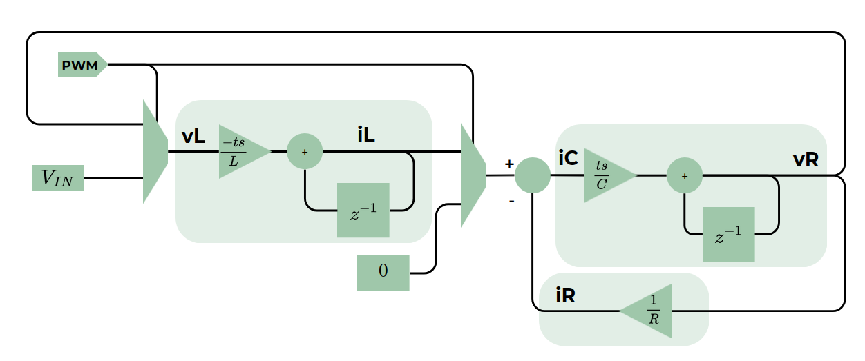
The negative output voltage comes from the inductor current, which flows in the opposite direction than the output current. The next figure shows the block diagram of the converter. In this case, we can find two multiplexers managed by the PWM input. The first multiplexers switch between the output voltage when the PWM signal is zero, and the input voltage when the PWM is active. The second multiplexer sets current through the diode, which is inductor current when the PWM is zero, and zero when the PWM signal is active.
The rest of the elements are the integrators for the inductor current and the capacitor voltage, and the division by the resistance of the load to calculate the output current. Notice that the integrators need to be multiplied by the time step.
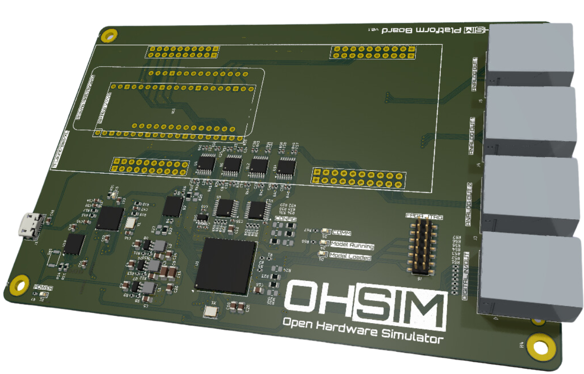
The model will be deployed on the OHSim Platform Board. Ths board features an AMD Spartan 7, 16 ch 12-bit analog outputs, and 12 digital inputs. The Platform Board is compatible with TI Launchpad. Raspberry PI Pico 1/2 and Arduino MKR and Portenta.
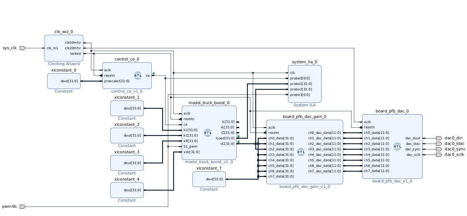
The project is implemented on Vivado using the next Block Design. We can see that the different parameters of the model are set using Constant blocks. Also, a control_ce block is added to generate the clock enable of the model, which is configured at 1 us. The outputs of the model are connected to the board_pfb_dac_gain block, which converts the 32-bit output of the model to a 12-bit signal, Finally, the outputs the the gain module are connected to the board_pfb_gain block, which is the DAC0 driver.
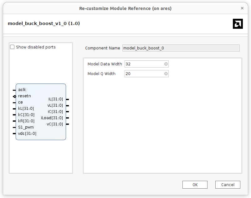
The module that implements the model of the converter can work with different fixed-point precisions. The configuration is given with parameters, so from the Blcok Design we can change the data width and the precision. Notice that these changes affect the values of the constants connected externally.
In the block design, we can also see that the PWM input used is the pwm4b input, and the capacitor voltage, which is also the output voltage of the model, is connected to channel number two of the DAC0 driver. This combination depends on the board we are going to use with the Platform Board. In this case, I have used an Arduino MKR to control the converter (yes, it is not the best choice, but it is the easiest to implement).
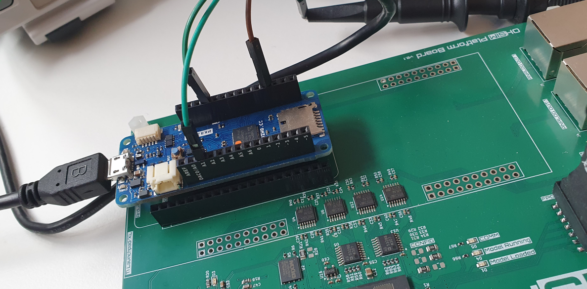
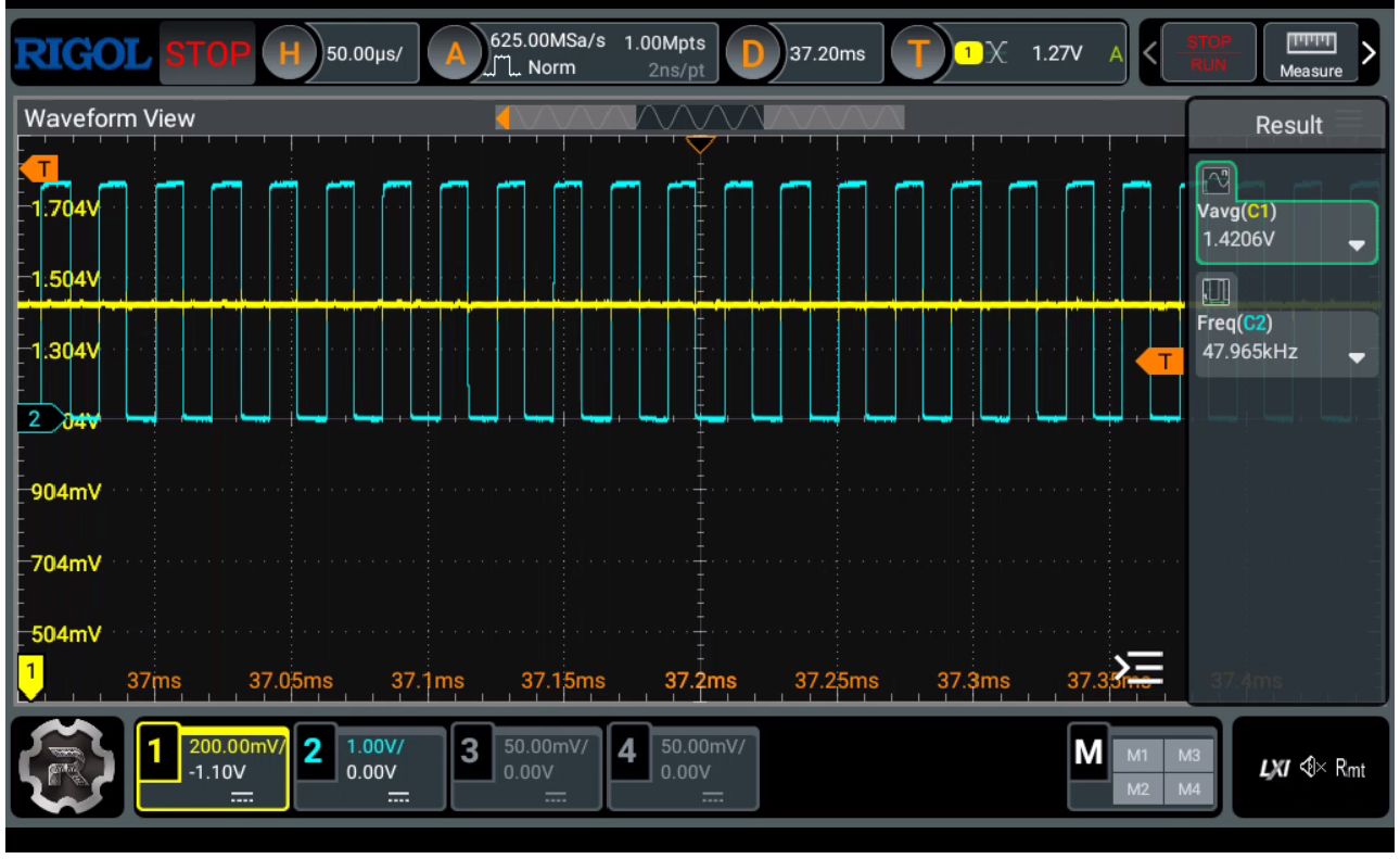
The pwm4b input is connected to the DIO 9 of the Arduino, which is a PIn able to generate high-frequency PWM signals. In this case is configured to 48 kHz. The channel 2 of the DAC0 is connected to the A1 pin of the Arduino, and it is able to reach a resolution of 12 bits. In the next scope capture, you can see the PWM frequency of the Arduino MKR. This frequency can be achieved in two ways, modifying the value of the timer and PWM registers manually, or using a third-party library like the SAMD21turboPWM.
Now, is turn for the acquisition. As I mentioned before, this output voltage is if the converter is connected to the pin A1 of the MKR. The ADC of the Arduino MKR, by default, has a reference of 3.3 volts. On the other side, we have the Platform Board DAC. This DAC works within a range of 0 - 3 volts, so to generate negative voltages I have to set an offset voltage in the middle of the range, in this case, a reading of 0 volts will be translated into 1.5 volts in the DAC channel. Also, in order to obtain the real volts of the converter, we have to pay attention to the precision of the model, this is, the data width, and the decimal data width. I have configured a data width of 32 bits, with a decimal part of 20 bits, which means an integer part of 12 bits. Since the DAC has also a resolution of 12 bits, the code that I am sending to the DAC is directly the real volts of the converter. With these parameters, we can translate the reading of the Arduino ADC to the volts of the converter.
voltage_adc = analogRead(A1)*3.30/4096;
voltage_signed = voltage_adc - 1.5;
voltage_real = voltage_signed * 4096/3;
To test this, we can control the converter in an open-loop using a fixed-duty cycle. Since this is an ideal model and has no losses, the open-loop voltage will follow the transfer function of the converter.
The converter’s input voltage is 100 volts, so for a duty cycle of 50%, the output of the converter would be -100 volts.
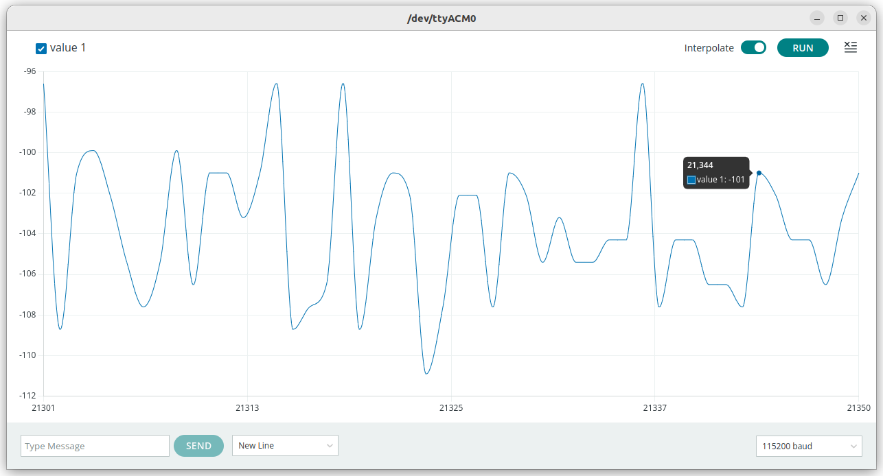
Now, we can implement a basic PI control in the Arduino MKR to check the behavior of the converter.
error = reference + voltage_real;
error_sum = error_sum + error;

proportional_control = kp*error;
integral_control = ki * error_sum;

control = proportional_control + integral_control;

/* saturation */
if (control > 900) control = 900;
if (control < 0) control = 0;
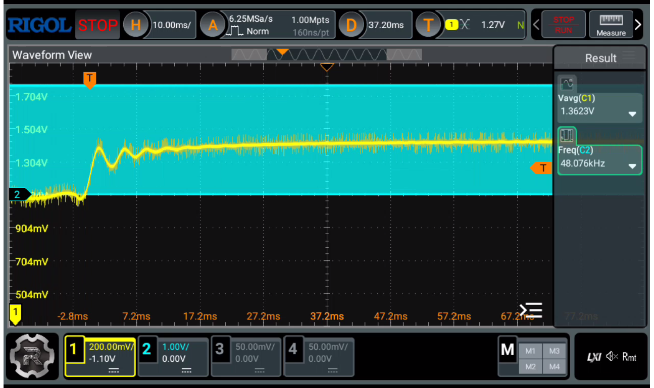
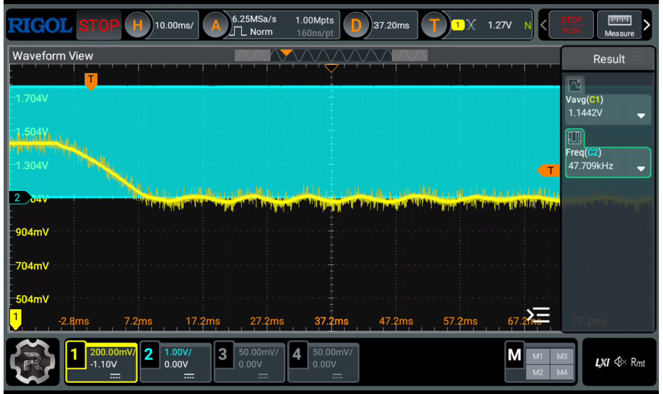
The controller will change the reference ever second from -100 to -550 volts. The next capture shows the output voltage of the converter from -550 volts to -100 volts.
Finally, the capture from -100 volts to -550 volts.
The amount of analog channels and digital inputs the Platform Board features allows us to implement more complex applications, for example, we can read the output current and implement an overcurrent protection, or even add the thermal model of the switch, which is essentially an energy meter in the switch will allow us to implement temperature protections. The choices that this kind of platform gives you are endless. The hardware of this platform is open source and it is able to be downloaded from GitHub. If you are brave enough, you can build your own on JLCPCB using all the output files released on the repository.


