Deploying a converter model on the Leonidas board
When discussing real-time simulations, we often think of big and powerful devices. In the same way, when we talk about Hardware-In-the-Loop (HIL), we think on FPGA like the Kintex7 used in the Speedgoat Performance so, do we need huge FPGAs to perform real-time hardware simulations? The short answer is no, the long one is, that it depends. Some factors make those manufacturers use big FPGA, and the first one is that a device like this must be capable of running from small to huge models, and, the larger the model, the larger the FPGA we need to deploy it but, does that means that we need big FPGA for every model?, absolutely no, so, if you want to learn how you can deploy a model in a $100 FPGA board, this article is for you.
The model we are going to deploy is a Boost converter, a step-up converter. We already obtained the RTL model of this converter in this article. In that article, we verified the model by performing some simulations. This time, we are going to verify the model deploying it on the Adiuvo’s Leonidas Board, a board based on the smallest AMD FPGA available, the Spartan7 XC7S6. This FPGA features just 10 DSP blocks and 6k logic elements, which, as we will see, is enough to deploy a small model.
The article is divided into three different parts.
- Creating the top module of the model.
- Simulation of the model.
- Deploying the model.
- Verify the model in a real-time simulation.
Creating the top module of the model.
As I mentioned before, we are going to use the model created in a previous article, but it is just the model, so we will need to develop the rest of the modules to make this model deployable on a real FPGA board.
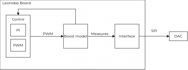
Since we will need to verify the entire design, to be sure that it works as expected, we are going to design two different top modules. The first one will be used for simulations and will involve all the modules needed to generate the PWM signal, the proportional-integral regulator, the external interface, and the model itself.
The second top module will be the one we will deploy on the board. This model will only contain the converter model and the external interface.
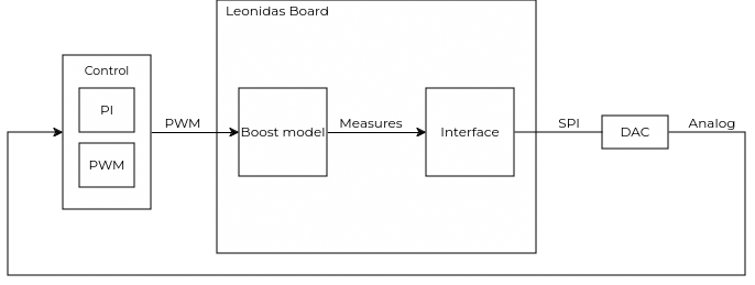
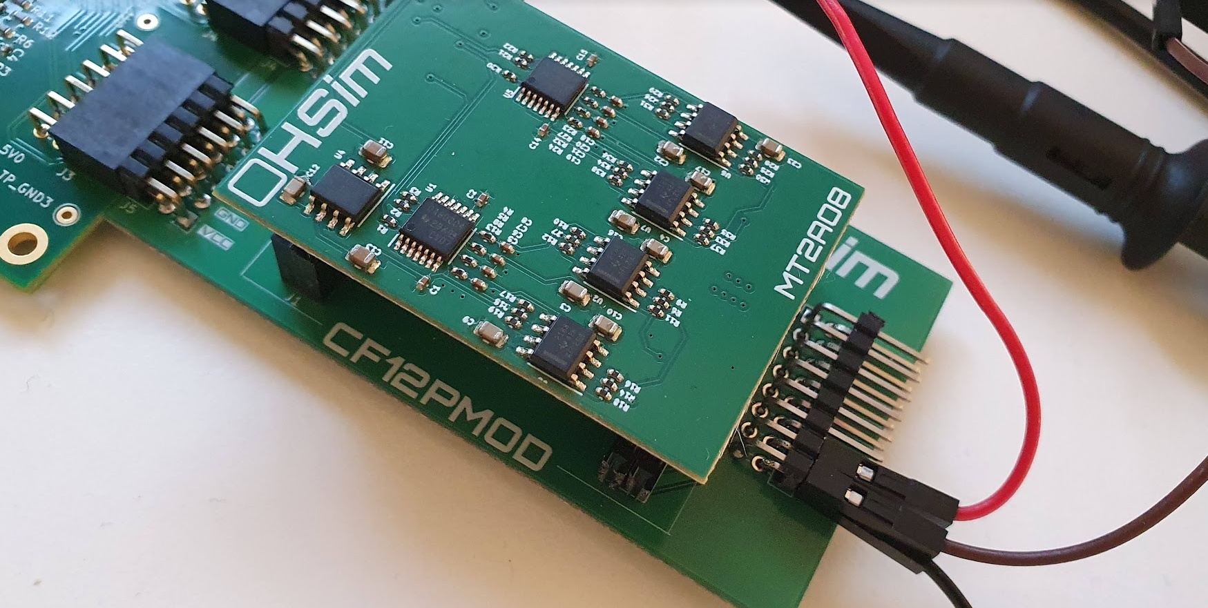
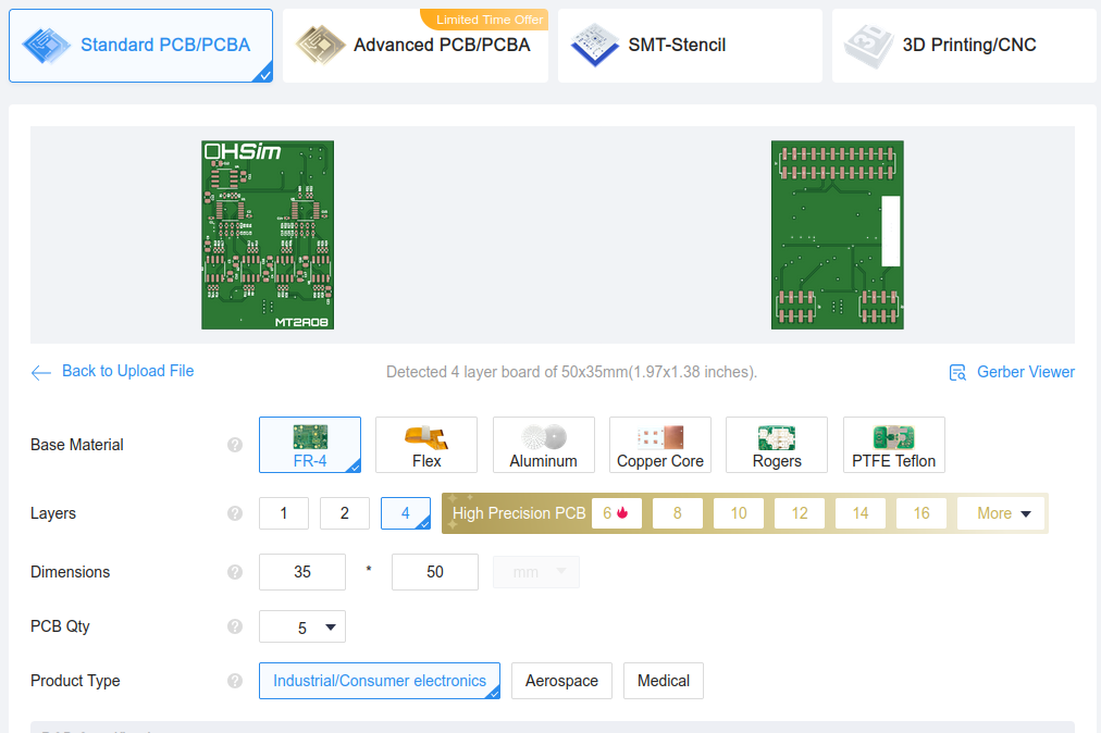
As an external interface, we will use the MT2AO8, a custom board designed for the project OHSim that features 2 DAC with 16-bit resolution and able to generate signals up to +-12V. This board is manufactured by JLCPCB. Obviously, for the simulation, we will only check that the SPI interface is working correctly.
To make the model deployable in a small FPGA, we need to make some modifications to the model. To avoid delays, in the original model, all the multiplications were made combinationally, this is, without using the registers of the DSP48 blocks. This creates long paths that generate large delays. Even reducing the clock frequency from 100 MHz to 50 MHz, the design timing constraints failed. To increase the speed of the model we need to add registers in the multiplications. By doing this, and with a clock frequency of 50 MHz, the design’s timing requirements are all met.
	/* input inductor voltage */
	always @(posedge aclk)
		vRL_k_ds <= $signed({ {DATA_WIDTH{iL[DATA_WIDTH-1]}}, iL} * { {DATA_WIDTH{kL[DATA_WIDTH-1]}}, kRL});
Regarding the top module of the design, I have used a `define to configure the top module for simulation, or deployment. For example in the model in/out configuration, for simulation, I have a clock generated in the testbench, so the clock is generated externally to the design, however, in the deployment, I have added a Clocking Wizard IP, so the clock is generated inside the top module. For simulation, it is fine to use Clocking Wizard IPs, but in this case, we need to simulate with Vivado, or any other simulator able to work with the IP sources. In my case, I use iVerilog, so I need to do this.
module leonidas_boost_top (
`ifndef SIMULATION
	input wire sys_clk,
	input wire control_pwm,
`else
	input wire aclk,
	input wire clk20mhz,
	input wire resetn,
`endif

	/* DAC interface */
	output wire spi_aclk,
	output wire spi_sync,
	output wire spi0_data,
	output wire spi1_data
	);
Since the model has no communication, all the parameters of the model are defined inside the top module.
/**********************************************************************************
*
* Model parameters
*
**********************************************************************************/
parameter DATA_WIDTH = 32; /* model data width */
parameter DECIMAL_DATA_WIDTH = 22; /* model data width */
parameter PWM_PERIOD = 32'sd1000; /* pwm period 50e3 = 100e6/x -> x=2000*/
parameter MODEL_REFERENCE = 65*(2**DECIMAL_DATA_WIDTH); /* 65 volts */
Here you can see the instantiation of the reset and the clock, according to the SIMULATION definition.
`ifndef SIMULATION
	clk_wiz_0 clock_inst (
  .clk100mhz(aclk),     // output clk100mhz
  .clk20mhz(clk20mhz),     // output clk20mhz
  .locked(clock_locked),       // output locked
  .clk_in1(sys_clk)      // input clk_in1
	);

	always @(posedge aclk)
		clock_locked_1 = clock_locked;

	assign resetn = &{clock_locked_1, clock_locked};

`endif
Again, if we are performing a simulation, all the control is inside the module and added according to the SIMULATION variable.
	/**********************************************************************************
	*
	* Control side
	*
	**********************************************************************************/
`ifdef SIMULATION
	pi_fixp #(
  .DATA_WIDTH(DATA_WIDTH),
  .DECIMAL_DATA_WIDTH(DECIMAL_DATA_WIDTH)
	) pi_regulator_inst0 (
  .aclk(aclk),
  .resetn(resetn),
  .ce(ce),
  .in(model_vC), /* feedback input */
  .reference(MODEL_REFERENCE), /* reference input */
  .kp(32'sd40), /* proportional constant input */
  .ki(32'sd200), /* integral constant input */
  .saturation_p(32'd1500000000), /* regulator positive saturation */
  .saturation_n({DATA_WIDTH{1'b0}}), /* regulator negative saturation */
  .out(pi_output_fixp)
	);

	assign modulator_comp = {22'd0, pi_output_fixp[28-:10]};

	modulator pwm_modulator_inst0 (
  .aclk(aclk),
  .resetn(resetn),
  .period(PWM_PERIOD),
  .comp(modulator_comp),
  .pwm(control_pwm)
	);
`endif
Finally, the converter model is added to the module. The values of the constants are fixed, and they can be calculated using a Python script. The model is executed with the time step of the ce signal. In this case, I have used a time step of 200 ns.
	/**********************************************************************************
	*
	* Plant side
	*
	**********************************************************************************/

	ohs_model_boost #(
  .DATA_WIDTH(DATA_WIDTH),
  .DECIMAL_DATA_WIDTH(DECIMAL_DATA_WIDTH)
	) boost_model_inst0 (
  .aclk(aclk),
  .resetn(resetn),
  .ce(ce),
  /* Model parameters */
  .kL(32'd20971),
  .kRL(32'd4194),
  .kC(32'd4194),
  .kR(32'd838860),
  .vdc(32'd209715200), /* 50 volts */
  /* PWM input */
  .S1_pwm(control_pwm),
  /* Model outputs*/
  .iL(model_iL),
  .vL(model_vL),
  .iC(model_iC),
  .vC(model_vC),
  .iLoad(model_iLoad)
	);
Finally, the interface instantiation. The MT2AO8 board features two DAC80004, so the mt2ao8_driver includes inside two drivers for that DAC. Also, it allows to apply a gain to the signal by adding a shift register to each signal. The SPI interface works at aclk divided by two.
	/**********************************************************************************
	*
	* Interface side
	*
	**********************************************************************************/

	mt2ao8_driver #(
	.MODEL_Q_WIDTH(DECIMAL_DATA_WIDTH),
	.CH0_SHIFT(0),
	.CH1_SHIFT(0),
	.CH2_SHIFT(0),
	.CH3_SHIFT(0),
	.CH4_SHIFT(0),
	.CH5_SHIFT(2),
	.CH6_SHIFT(0),
	.CH7_SHIFT(0)
	) dac_inst0 (
	.aclk(clk20mhz),
	.resetn(resetn),
	/* Analog outputs values */
	.ch0(model_iL),
	.ch1(model_vL),
	.ch2(model_iC),
	.ch3(model_vC),
	.ch4(model_iLoad),
	.ch5(pi_output_fixp),
	.ch6(32'd0),
	.ch7(32'd0),
	/* External interface */
	.spi_aclk(spi_aclk),
	.spi_sync(spi_sync),
	.spi0_data(spi0_data),
	.spi1_data(spi1_data)
	);
Once we have the top module ready, we can jump to the simulation stage.
Simulation of the model.
I like to make all the simulations using scripts. This allows me to be able to repeat the simulation always under the same conditions, as well as execute the same simulation on any computer. The script I used for this simulation is the run.sh. Notice that I have added the -DSIMULATION argument, which is equivalent to adding in the top module define SIMULATION.
#!/bin/bash

SOURCE="../src/cen_generator.v ../src/dac_controller.v ../src/leonidas_boost_top.v ../src/modulator.v ../src/mt2ao8_driver.v ../src/ohs_model_boost.v ../src/pi_fixp.v"
TEST_SOURCE="./leonidas_boost_tb.sv"
TOP_MODULE="leonidas_boost_tb"

iverilog $SOURCE $TEST_SOURCE -s $TOP_MODULE -g2005-sv -DSIMULATION -o sim.vvp
vvp sim.vvp
rm ./sim.vvp
In this simulation, I started with a reference of 65 volts, with an input voltage of 50 volts. Then, at 10ms, the reference changes to 85 volts. Executing this script, and visualizing data with GTKWave, the result is the next.
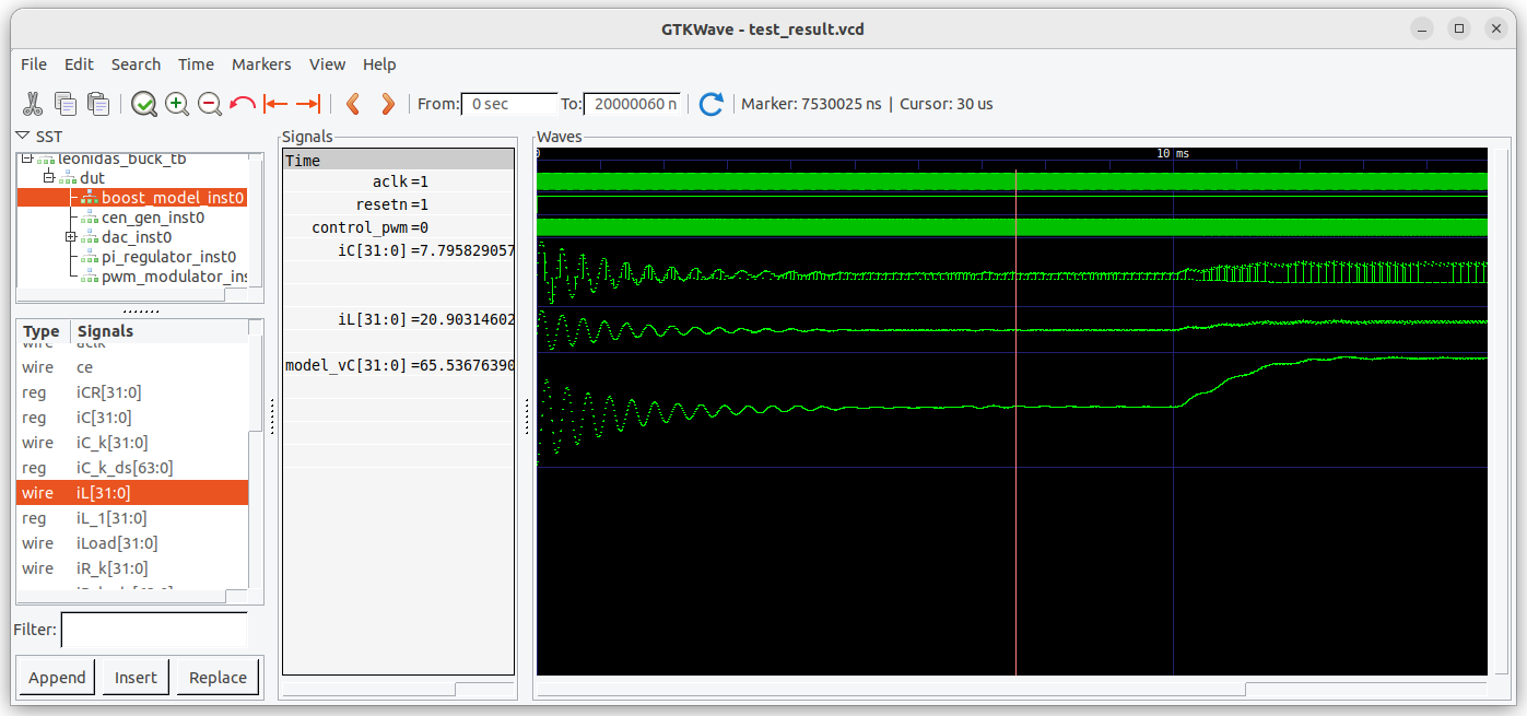
At this point we know that the top module and the model works as expected, so it is time to deploy the model on the Leonidas board.
Deploying the model.
To deploy the model we need to launch an implementation. On the first try, these were my results.
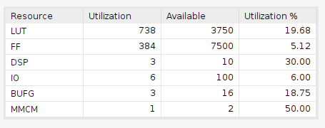

Since the converter model has 4 multiplications of 32 bits each one, I expected to use eight multiplicators (two per multiplication). However, we can see that the amount of DSP48 blocks is just three. This means that Vivado is using regular logic to implement multiplicators. This will work, but it is not what we want because the paths will be larger, and the design will be slower.
To force Vivado to use the DSP48 blocks for the multiplications, we can add (* use_dsp = "yes" *) just above the converter module declaration. Doing this, we have the next results.
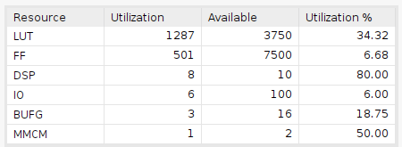

In this case, we can see how the amount of DSP blocks is eight, which is what we expect. However, the amount of logic used has been increased because of the logic added between DSP blocks and the paths generated to connect all the DSP blocks. Also, we can see that using DSP48 blocks, makes our design faster, reducing the WNS to half.
Now, it’s time to configure the FPGA and test the model.
Verify the model in a real-time simulation.
To verify the model I used the Leonidas Board and the MT2AO8 board with an oscilloscope. To generate the PWM signal, I added a PWM generator in the top module since I do have not an ADC board to connect to another FPGA. The PWM module generates two different PWM signals with different duty cycles, making the output voltage increase and decreasing.
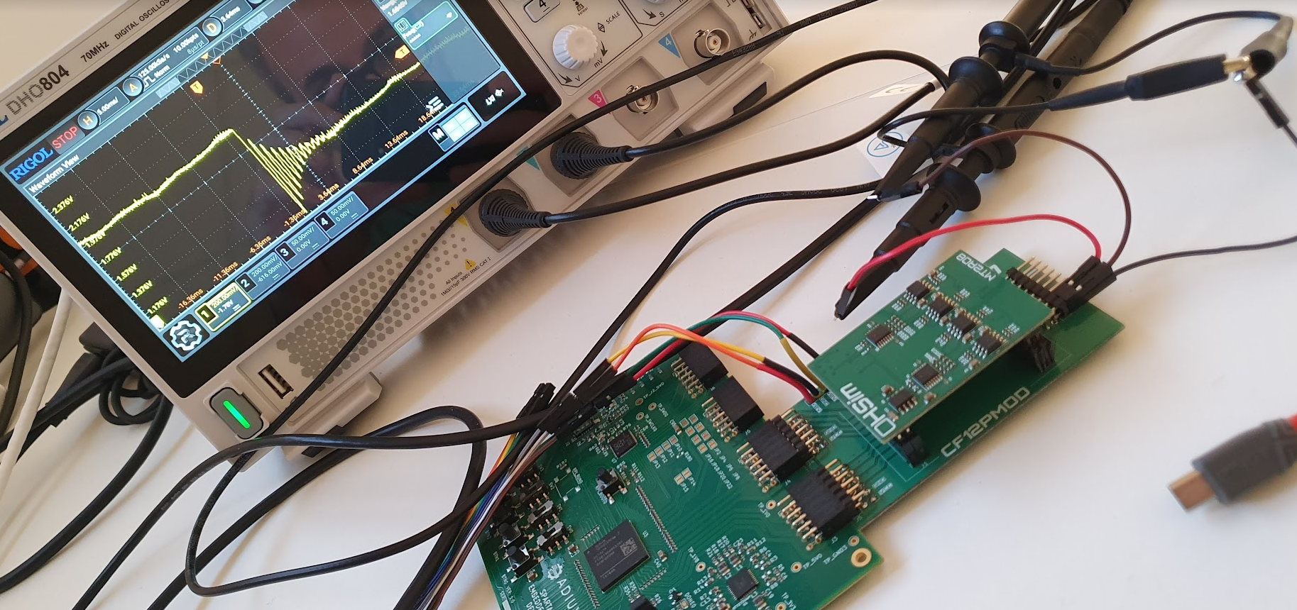
In the next capture, we can see the step down of the duty cycle, with the resonance of the model.
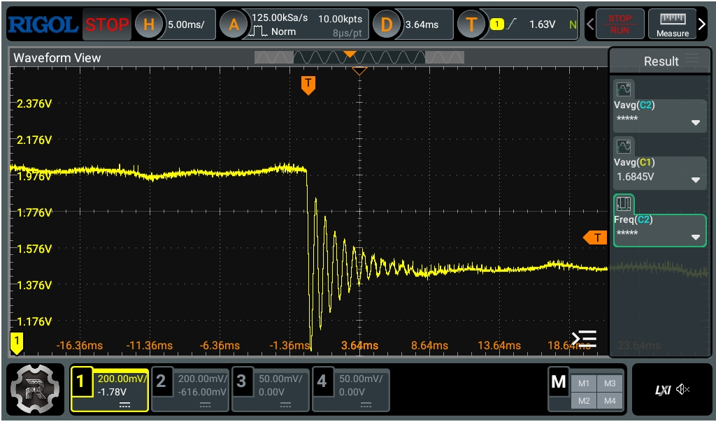
In the next capture, we can see the step up, also with the corresponding resonance of the LC filter.
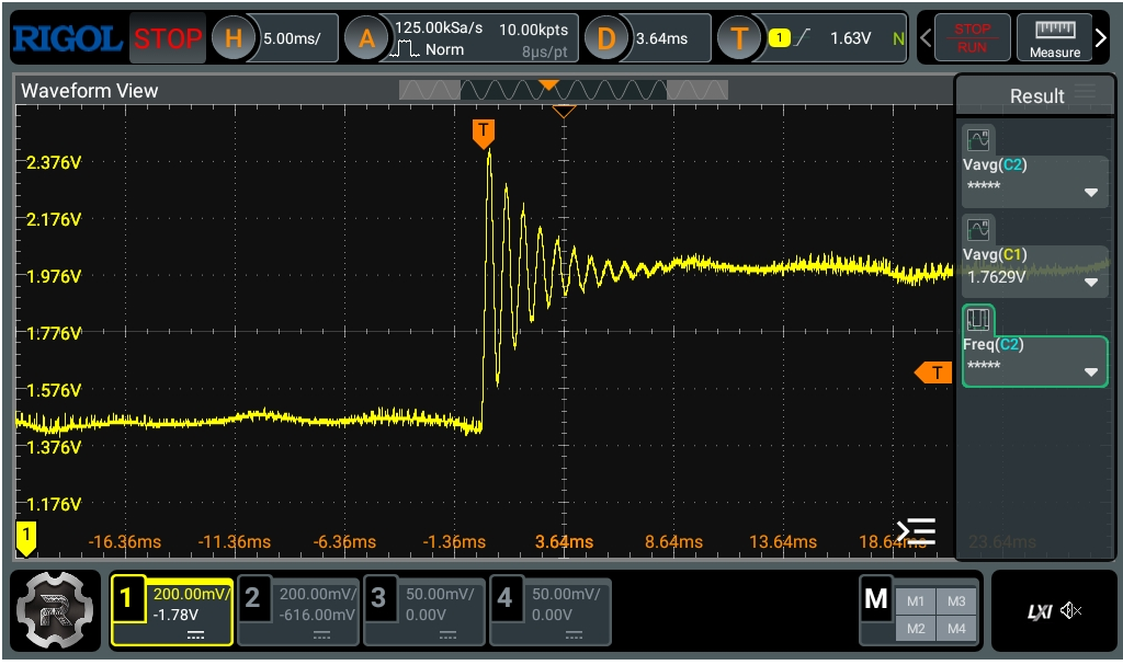
So, to the question, do we need huge FPGAs to perform real-time hardware simulations? we can see that for a Boost converter, the answer is no. And this is valid for many other converters that we will deploy soon on small FPGAs. Imagine the model we can deploy of boards like the ZUBoard, which features a Zynq MPSOC with 81k logic cells and 216 DSP blocks.
I am working on custom hardware which will be released soon, for now, if you want to make your own MT2AO8, you can check its repository, and go to JLCPCB to get your own.
Keep connected to OHSIM.tech


